
We all know that Samsung makes some of the best smartphones on the market, but many users often prefer the Qualcomm chips over the Exynos variants as they’re more powerful and efficient. That, however, doesn’t stop Samsung from innovating and working on new fabrication processes, and it developed a new 3nm technology, paving the way for new more powerful, and more efficient chips to be manufactured at its facilities.
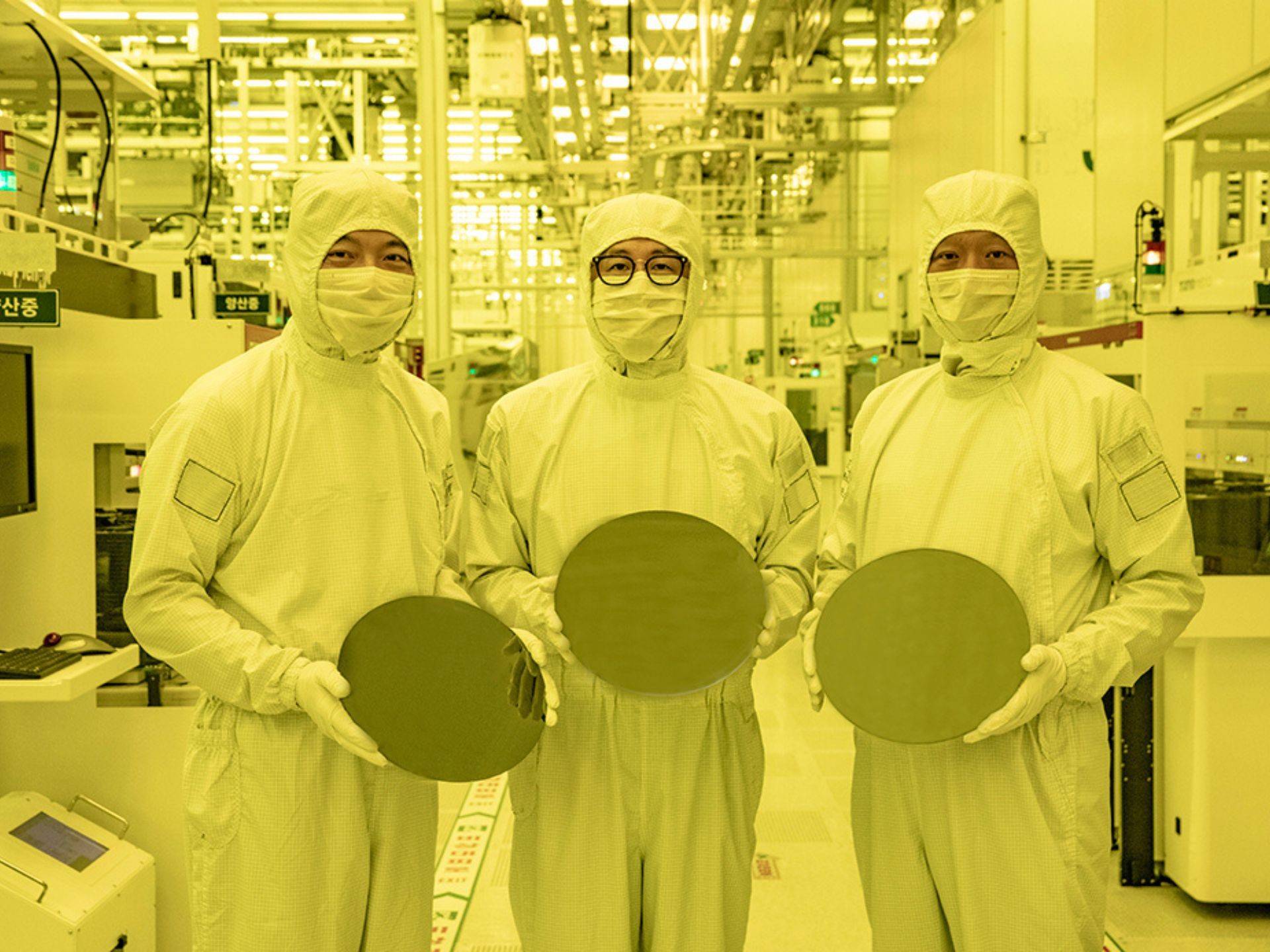
Samsung Foundry announced its beginning mass production of first-generation chips, based on the 3nm technology. The new chips will be based on the new Gate-All-Around (GAA) transistor architecture, replacing the previous FinFET. The new 3nm technology will offer significant improvements compared to the 5nm technology, namely a 23% performance update, and the chip will be up to 45W more power-efficient. The chip is also 16% smaller.
“Optimized 3nm process achieves 45% reduced power usage, 23% improved performance and 16% smaller surface area compared to 5nm process”
The first-generation 3nm chips will initially be available for high-performance, low-power computing devices, but Samsung plans to expand it to mobile processors in the future. We look forward to seeing how this develops over the coming months and years, and we’re excited to see the doors this new technology opens for smartphones, tablets, and computers.
How does it work?

Samsung explains that the new proprietary technology utilizes nanosheets with wider channels, allowing for higher performance and greater energy efficiency compared to GAA technologies using nanowires with narrower channels. The new 3nm GAA technology will allow Samsung to adjust the width of the nanosheet to optimize the power usage and performance, increasing the power output and significantly improving the efficiency.
The company also said that the new GAA architecture offers more design flexibility, allowing for greater benefits for optimizing the power and boosting performance. The second-generation 3nm process is expected to reduce the power consumption by up to 50% while improving the performance by 30% in a 35% smaller area. These results are impressive, and appear to be better than the annual upgrades we see in chipsets, although the real-world use will likely differ based on the operating system and the purpose they’re used for.
What are the benefits?

As mentioned above, Samsung claims to achieve 45% reduced power usage, 23% improved performance on a 16% smaller surface area, compared to the 5nm process. These numbers suggest that real-world applications will benefit greatly from the new architecture and the new process, proving to be better for all kinds of applications.
Smartphones, computers, tablets, and other devices will benefit from the new technology as they will be able to pack more power in a smaller area. As the power increases, the efficiency will also grow higher, making the devices last longer, while consuming less power. The functionality of these chips will also become more extensive, and OEMs will be able to offer more hardware and software features as a result.
Current high-end smartphones have 4nm processors, such as the Qualcomm Snapdragon 8 Gen 1 SoC. These chips are already powerful and efficient, but there’s always room for improvement. Semiconductor factories, such as TSMC, are also working on delivering 3nm chips sometime this year, and it appears like Samsung managed to take over and announce the technology first. TSMC, and other semiconductor companies are also heavily investing in 2nm fabrication processes, and they will likely be available in the coming years, offering even better efficiency and performance.
Samsung is expected to begin the mass production of 3nm chips in the second half of 2022, and we could see new computing applications arrive with the new chips soon. It’s unclear what devices will receive it first, and we’re unlikely to see new devices equipped with such chips this year.


